- 您现在的位置:买卖IC网 > Sheet目录365 > TC4432VOA713 (Microchip Technology)IC MOSFET DRIVER 30V 1.5A 8SOIC
�� �
�
�TC4431/TC4432�
�3.0�
�PIN� DESCRIPTIONS�
�The� descriptions� of� the� pins� are� listed� in� Table� 3-1� .�
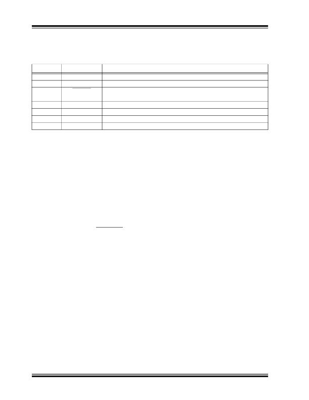
�TABLE� 3-1:�
�PIN� FUNCTION� TABLE�
�Pin� No.�
�1�
�2�
�3�
�4�
�5�
�6�
�7�
�8�
�Symbol�
�V� DD�
�IN�
�LOCK� DIS�
�GND�
�GND�
�OUT�
�OUT�
�V� DD�
�Description�
�Supply� Input,� 4.5V� to� 30V�
�TTL/CMOS� Compatible� Input�
�Input� Pin,� Enable/Disable� for� UV� Lockout�
�Ground�
�Ground�
�Drive� Output,� Pull� Down�
�Drive� Output,� Pull� Up�
�Supply� Input,� 4.5V� to� 30V�
�3.1�
�Supply� Input� (V� DD� )�
�3.4�
�Ground� (GND)�
�The� V� DD� input� is� the� bias� supply� input� for� the� MOSFET�
�driver� and� is� rated� for� 4.5V� to� 30V� with� respect� to� the�
�ground� pins.� The� V� DD� input� should� be� bypassed� to�
�ground� with� a� local� ceramic� capacitor.� The� value� of� this�
�capacitor� should� be� chosen� based� on� the� capacitive�
�load� that� is� being� driven.�
�The� ground� pins� are� the� return� path� for� the� bias� current�
�and� for� the� high� peak� currents� which� discharge� the� load�
�capacitor.� Both� ground� pins� should� be� used� to� ensure�
�proper� operation.� The� ground� pins� should� be� tied� into� a�
�ground� plane� or� have� short� traces� to� the� bias� supply�
�source� return.�
�3.2�
�Control� Input� (IN)�
�3.5�
�Drive� Output� (OUT)�
�The� MOSFET� driver� input� is� a� TTL/CMOS� compatible�
�input� with� 250� mV� of� hysteresis� between� the� high� and�
�low� threshold� voltages.� If� an� input� signal� level� of� greater�
�than� 12V� is� applied� to� the� device,� a� series� current�
�limiting� resistor� is� recommended.�
�The� TC4431/TC4432� devices� have� individual� source�
�and� sink� output� pins.� This� feature� can� be� used� to� adjust�
�the� rise� and� fall� time� independently� by� adding� separate�
�charge� and� discharge� resistors� external� to� the� device.�
�Pin� 7� (source� output)� can� source� 3� A� peak� currents� into�
�capacitive� loads� and� pin� 6� (sink� output)� can� sink� 1.5� A�
�3.3�
�Lockout� Disable� (LOCK� DIS)�
�peak� currents� from� a� capacitive� load.�
�The� lockout� pin� enables/disables� the� undervoltage�
�lockout� feature� of� the� device.� If� undervoltage� lockout� is�
�desired� (output� is� not� enabled� until� the� bias� voltage�
�reaches� 8.4V� (typical)� on� the� rising� edge� and� is�
�disabled� when� the� bias� voltage� reaches� 7.7V� (typical)�
�on� the� falling� edge),� the� lockout� pin� should� be� left� float-�
�ing.� If� operation� below� 7V� is� desired,� the� lockout� pin�
�should� be� tied� to� ground.�
�DS21424D-page� 6�
�?� 2007� Microchip� Technology� Inc.�
�发布紧急采购,3分钟左右您将得到回复。
相关PDF资料
TC4452VPA
IC MOSFET DVR 12A HS 8DIP
TC4467COE
IC MOSFET DVR QUAD NAND 16SOIC
TC4627EOE
IC MOSFET DRIVER 1.5A 16SOIC
TCN1.25SV
THERMASHIELD CONVOLUTED 1.25" 4'
TCSD-12-01-N
CONN SOCKET 24 POS 2MM GOLD
TDGL004
BOARD CEREBOT 32MX7 PIC32MX795
TEACLIPPER-PIC-HV-PT
PROGRAMMER TEACLIPPER/PIC HI-V
TJA1010T/N1,118
IC OCTAL LOW SIDE DRVR 28SOIC
相关代理商/技术参数
TC4432VPA
功能描述:功率驱动器IC 1.5A Sngl 30V MOSFET Drvr N-Inv RoHS:否 制造商:Micrel 产品:MOSFET Gate Drivers 类型:Low Cost High or Low Side MOSFET Driver 上升时间: 下降时间: 电源电压-最大:30 V 电源电压-最小:2.75 V 电源电流: 最大功率耗散: 最大工作温度:+ 85 C 安装风格:SMD/SMT 封装 / 箱体:SOIC-8 封装:Tube
TC4451
制造商:MICROCHIP 制造商全称:Microchip Technology 功能描述:12A High-Speed MOSFET Drivers
TC4451VAT
功能描述:功率驱动器IC 12A Sngl MOSFET Drvr RoHS:否 制造商:Micrel 产品:MOSFET Gate Drivers 类型:Low Cost High or Low Side MOSFET Driver 上升时间: 下降时间: 电源电压-最大:30 V 电源电压-最小:2.75 V 电源电流: 最大功率耗散: 最大工作温度:+ 85 C 安装风格:SMD/SMT 封装 / 箱体:SOIC-8 封装:Tube
TC4451VMF
功能描述:功率驱动器IC 12A Sngl MOSFET Drvr RoHS:否 制造商:Micrel 产品:MOSFET Gate Drivers 类型:Low Cost High or Low Side MOSFET Driver 上升时间: 下降时间: 电源电压-最大:30 V 电源电压-最小:2.75 V 电源电流: 最大功率耗散: 最大工作温度:+ 85 C 安装风格:SMD/SMT 封装 / 箱体:SOIC-8 封装:Tube
TC4451VMF713
功能描述:功率驱动器IC 12A Sngl MOSFET Drvr RoHS:否 制造商:Micrel 产品:MOSFET Gate Drivers 类型:Low Cost High or Low Side MOSFET Driver 上升时间: 下降时间: 电源电压-最大:30 V 电源电压-最小:2.75 V 电源电流: 最大功率耗散: 最大工作温度:+ 85 C 安装风格:SMD/SMT 封装 / 箱体:SOIC-8 封装:Tube
TC4451VOA
功能描述:功率驱动器IC 12A Sngl MOSFET Drvr RoHS:否 制造商:Micrel 产品:MOSFET Gate Drivers 类型:Low Cost High or Low Side MOSFET Driver 上升时间: 下降时间: 电源电压-最大:30 V 电源电压-最小:2.75 V 电源电流: 最大功率耗散: 最大工作温度:+ 85 C 安装风格:SMD/SMT 封装 / 箱体:SOIC-8 封装:Tube
TC4451VOA
制造商:Microchip Technology Inc 功能描述:MOSFET Driver IC
TC4451VOA713
功能描述:功率驱动器IC 12A Sngl MOSFET Drvr RoHS:否 制造商:Micrel 产品:MOSFET Gate Drivers 类型:Low Cost High or Low Side MOSFET Driver 上升时间: 下降时间: 电源电压-最大:30 V 电源电压-最小:2.75 V 电源电流: 最大功率耗散: 最大工作温度:+ 85 C 安装风格:SMD/SMT 封装 / 箱体:SOIC-8 封装:Tube